Materials and Nanoscience Facilities
-
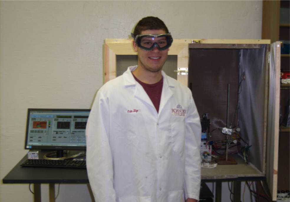
The lab currently houses a Chemical Vapor Deposition (CVD) system for the growth of carbon nanotubes. It is used for fabrication of nanotube-based sensor devices and smart coatings. Nanophased iron oxides using wet chemical methods are also been synthesized.
The research projects currently being pursued are synthesis of nanophased iron oxides, growth of single-wall carbon nanotubes from patterned nanocatalyst arrays, analysis of Mossbauer spectroscopic data from planet Mars and fabrication of nano-sensor devices and smart coatings.
-
The Physics Group has purchased a high resolution atomic force microscope (AFM). This instrument can produce high resolution images of structures that are 1000 times smaller than a human hair. Physics students and faculty use the AFM for mapping micro and nanostructures, studying surface properties of thin films, and manipulating matter at the nanoscale.
-
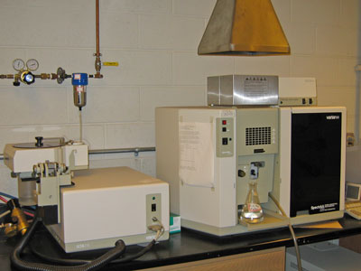
Our fluorescence spectrometer is used to detect trace levels of fluorescent molecules, down to 0.000000000001 moles/liter.
-
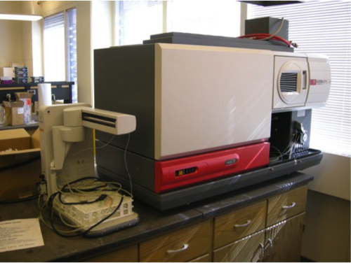
Atomic spectroscopy measures metals in environmental samples at the ppm and ppb levels.
-
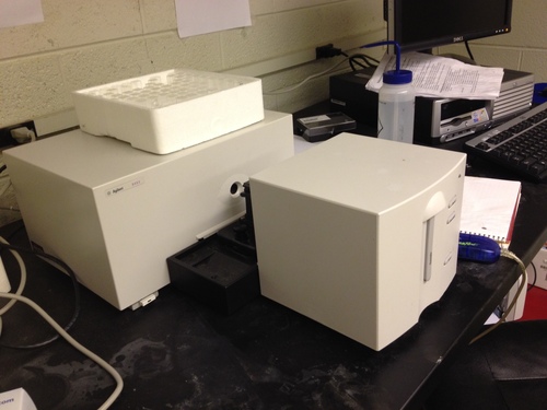
Our diode array UV-visible spectrometer can collect a complete spectrum in just a few seconds. .
-
FSCV (Fast-Scan Voltammetry) is an electrochemical technique that allows for the nonomolar-level detection of several species including catecholamine neurotransmitters.
-
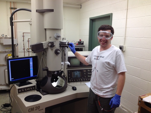
The Transmission Electron Microscope (TEM) is the most powerful tool for the materials chemist, allowing us to image our crystals down to the sub-nanometer level. In some cases we can even resolve the packing of the atoms within an individual crystal.
-
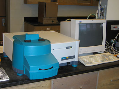
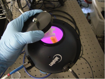
Fluorescence - Many of our crystals are highly fluorescent, which is particularly important when we hope to use these for LED phosphors. Our group's fluorimeter with integrating sphere (shown above), allows us to quantatatively determine a sample's absorption/emission efficiency known as the quantum yield.
-
The UV/Vis Absorption allows us to measure how well our nanocrystals absorb light in the ultraviolet and visible spectrum. This is important since as phosphors, the crystals need to strongly absorb the light coming off of the underlying LED, which is commonly about 455 nm.
-
Inudctively Coupled Plasma (ICP) uses an argon plasma torch of roughly 10,000 degrees Celsius to atomize and excite a sample. It then detects the emission from the excited atoms to determince what elements are present in a sample. When calibrated, we can use ICP to determine the composition of our nanocrystals.
-
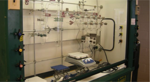
The Schlenk line - This fancy piece of glassware (pictured here inside a fume hood), allows us to easily switch between vacuum and a working gas (usually nitrogen), so that we may grow our crystals in an air-free environment. Both oxygen and water can adversely affect growth, so it's important that we remove as much as possible in our reaction process.